The GARP Power Subsystem Monitor (PSM) is a modular hardware and firmware component designed to provide visibility into the voltages and currents present across the Ground Autonomy Research Platform’s power rails. Its primary goals are to support system health monitoring, identify potentially problematic operating conditions, and simplify troubleshooting by correlating power behavior with subsystem activity. The PSM uses a motherboard–daughtercard architecture to monitor backend, intermediate, and frontend power rails, digitizing analog measurements via a multichannel ADC (MCP3008) and reporting data to the Command and Data Handler (C&DH) via a custom API. This article documents the design assumptions, electrical architecture, PCB implementation, and physical integration of the PSM, with an emphasis on modularity, scalability, and safe measurement of high-voltage and high-current rails. Circuit and PCB files for KiCad are available on GitLab at https://gitlab.com/mvstinger1/ground-autonomy-research-platform/garp-electrical-engineering, and CAD files in FreeCAD are available on GitLab at https://gitlab.com/mvstinger1/ground-autonomy-research-platform/garp-cad.git.
GARP Article Series
The Ground Autonomy Research Platform (GARP) is a home-grown UGV designed and built to support independent learning of robotics and autonomy through a full stack from hardware to behavioral autonomy and HMI. To document the implementation of GARP, I’m capturing the process in a series of articles that I’ll link here as they’re completed:
GARP Article Map
- Motivations and Design of a UGV for Robotics Research
- GARP Power Subsystem
- GARP Mobility Subsystem
- Motor Selection
- Subsystem Design
- Motor Controller
- C&DH
- Design
- Alpha Implementation
- GARP E-Stop
- Design
- Alpha Implementation
Objectives
The primary motivation behind the power subsystem monitor (PSM) is to provide enough visibility into the voltages and currents in play in the GARP to monitor system health, identify problematic situations, and ease troubleshooting:
- System Health: This can be as simple as seeing battery voltage for the sake of estimating remaining life or as complex as sampling voltage decline to produce a regression model and provide live runtime projections.
- Problematic Situations: As the power subsystem is involved in nearly every other component in the GARP, a number of different situations can arise that will can cause problems small or large. While several layers of protection are in place to avoid catastrophic issues (e.g. built-in battery protection circuits and breakers), having visibility into the strains such as current draw on batteries during behaviors can help inform soft limits extending the longevity of the GARP.
- Ease Troubleshooting: As more and more components are introduced and dependent on the power subsystem, the ability to correlate actions and effects across subsystems and components will make troubleshooting easier. For example, if a sudden motor velocity change causes a voltage dip that then causes another component to drop out, having log information from the power subsystem will help identify the issue.
To achieve this objective, this article will capture the design and implementation of a component dubbed the GARP power subsystem monitor (PSM) to monitor electrical power performance within the scope of the power subsystem. This includes the voltage and current on the power subsystem-supplied rails as well as battery data in future versions of the PSM. This would not include voltage and current draw of individual consumers of electrical power, such as the command and data handler (C&DH) or individual motors, which would be handled within their respective subsystems. As with most of the GARP, modularity should be baked-in to ease future development and flexibility.
Requirements
On a more general level, the PSM will need to support monitoring current and voltage across any voltage rails introduced on the GARP which means to avoid constant re-engineering and board spins, the design will need to be modular. The PSM will also need to report its measurements to the Command and Data Handler (C&DH) for further dissemination via the (e.g.) web interface. As a final general requirement, the PSM should introduce additional capacity where possible to best support growth (whether that’s via additional voltage rails or new functionality). To physically integrate with the rest of the GARP’s internals, the PSM should mount to a DIN rail.
Design Assumptions
More specifically, the baseline GARP design includes a backend 80 V power source, 24 V intermediate voltage (IV), and 5 V and 12 V frontend (FE) rails. To estimate the minimum currents drawn by the GARP and help inform the resolutions needed, consider the current drawn by the C&DH, four motor controllers, and the power monitor itself:
| Role | Part | Minimum Power Consumption |
| (Command and Data Handler) C&DH | Raspberry Pi 5 | 4.1 W 1 |
| Motor Controller | Raspberry Pi Pico2 | 30 mW 2 |
| Power Subsystem Monitor (PSM) | Raspberry Pi Pico2 | 30 mW 3 |
| 4.16 W Total |
Based on these ~rough~ numbers, the minimum total power consumption would be 4.25 W. This power consumption would amount to a certain draw on each rail, assuming the PSM is powered from the 5V rail itself:
| Rail | Voltage | Current |
| 80 V (Backend) | 50-82 V | 50 mA – 20 A 4 |
| 24 V (IV) | 24 V | 175 mA – 12.5 A 5 |
| 12 V (FE) | 12 V | 0 – 5 A 6 |
| 5 V (FE) | 5 V | 0 – 6 A 7 |
Beyond the resolution required of the PSM, the PCBs comprising the PSM must have adequate traces to support the maximum currents passing through the shunt resistors used to measure current consumption. This will be evaluated during design of each of the daughtercards.
Finally, note that I’ve assumed a Pico2 for the PSM microcontroller since they’re cheap, have SPI and I2C communications, and I’ve got a handful available. Also note that sampling rates on the order of 10 Hz are adequate- while this won’t allow characterizing transients, it will be adequate for capturing the steady-state operating points in scope for the PSM.
Design
At the top level, the PSM can be designed to use rail-specific daughtercards that plug into a motherboard. This not only supports modularity, but also means higher powers and thicker 3 oz copper can be kept to specific daughtercards, and can be isolated with (e.g.) optocouplers.
The first design choice is if the backend’s power and resistance measurements should be on a single daughtercard or if they should be broken out. Breaking them out (at least initially) will simplify layout, and will allow the design to keep the high power components separate from the low power resistance measurement. This will also mean only the backend’s power daughtercard will need the thickest copper traces.
The use of a motherboard and daughtercards configuration then introduces the question of an analog or digital interface. While a digital connection from daughtercard to motherboard could be made more robust via subsequent signal conditioning, the PSM is expected to be fairly compact (on the scale of a few inches) and so shouldn’t have trace lengths long enough to incur significant noise. Furthermore, using an analog interface means that the ADC can be on the motherboard, allowing use of a multichannel ADC like the MCP3008. One limitation of using an analog interface however, is that I cannot multiplex several signals onto the interconnect line like would be possible with an SPI bus line (neglecting a more exotic analog protocol). As a starting point, consider a four-pin analog connector between the motherboard and daughtercards:
| Pin | Function |
|---|---|
| 5 V | Power from motherboard |
| V1 | Channel 1 (e.g. Rail voltage) |
| V2 | Channel 2 (e.g. Rail current) |
| GND | 0 V reference from motherboard |
The daughtercard’s largest component is likely to be the input connection terminal. I’d like to use push-in terminals as they work well with the ferrules I’m using on the GARP and can be manipulated from the same face the wire is inserted into. If I stack the daughtercards, the terminal then sets the vertical spacing as well as the position of the connections to the motherboard- Note this still leaves the horizontal dimension of the daughtercard open for expansion. Staying to a single rail per daughtercard, this means I’ll need 2x 80 V, 2x 24 V, and 12 V and 5 V cards, for a total of 6 cards, not including a card for battery resistance.
Motherboard
From the discussion above, the motherboard will provide daughtercards with 5V and ground power connections and accept two analog signal lines each. Furthermore, the motherboard will host the microcontroller and ADC(s) to digitize the analog signals coming from the daughtercards. Given that at least 12 independent analog channels (2 analog signals per each of six daughtercards), two 8-channel MCP3008 ADCs would be required, while also leaving 4 channels open for future expansion (or a total of 8 daughtercards).
From the data sheet, the MCP3008 is an 8-channel 10-bit sample and hold ADC. The device supports 3.3V supply operation, and outputs digitized data via SPI which the Pico2 microcontroller also supports. It has a sampling rate upwards of 75 kSps, which is far greater than expected to be needed for the PSM. If we assume the analog signalling between the daughtercards and motherboard is in a 0-3.3 V range, the 10-bit resolution amounts to 1024 intervals or 3.2 mV resolution.
The Pico2 uses 3.3 V SPI, and the MCP3008’s SPI voltage is determined by the VDD supplied, meaning either the MCP3008 should be supplied 3.3 V directly, or a 5 V VDD should be used with a level shifter. This does mean that 3.3V will need to be produced alongside the 5 V for the daughtercards, but the MCP3008’s typical 300 uA current consumption is well within the ability of the Pico2’s power regulator to supply. Considering SPI speed, when operating in SPI controller mode, the Pico2’s data sheet (section 12.3.4.4) lists the maximum clock rate is 75 MHz, which is well above anything we should need. The MCP3008’s SPI speed is set via the SSPCPSR and SSPCR0 registers, up to 150 MHz, again significantly more than required for the PSM.
In a sample-and-hold ADC like the MCP3008, sample resolution is potentially impacted by the SPI clock rate. Footnote 2 to Table 6-1 in the MCP3008 datasheet 8 recommend an SPI clock rate of 2.34 MHz (resulting in a sampling rate of 130 kSps), but does not specify the maximum impedance fed to the ADC to support this recommendation. Drawing a line between the knees in the two given curves of Figure 4-2 puts the first tertile (3.3 V) at roughly 1 k of input impedance before the maximum clock frequency drops below 2 MHz. Once implemented there will be some flexibility in choosing the SPI clock rate as a function of performance, and first-order errors can be mitigated through bias and scaling in firmware.
Generic Daughtercard Design
The motherboard-daughtercard interface and an envelope of physical dimensions will define a sort of template for the daughtercards. Firstly, each of the daughtercards will have four connections to the motherboard: Two for 5 V power and ground supplied by the motherboard, and two providing analog voltage signals from the daughtercard to the motherboard. Secondly, as mentioned previously, the largest component on the daughtercard is expected to be the terminal block used to accept an input connection for each rail.
In general, each daughtercard will be responsible for measuring the voltage on the rail and the current consumed by it and encoding these measures on analog voltages to be provided to the motherboard. These two functions may be satisfied by single element such as a concurrent voltage and current monitoring IC or may require separate components and board space. This will be determined on a rail-by-rail basis in the design of each daughtercard.
The choice of connection between the daughtercard and motherboard has a vast array of options, from a simple board edge connector akin to peripheral component interconnect (PCI) cards, a through-hole post connector, or mezzanine connectors:
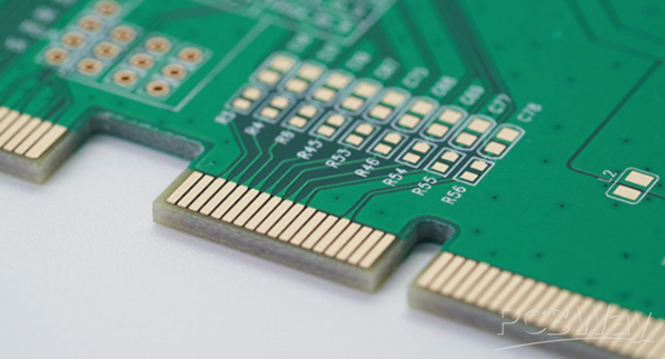
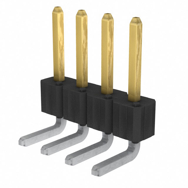
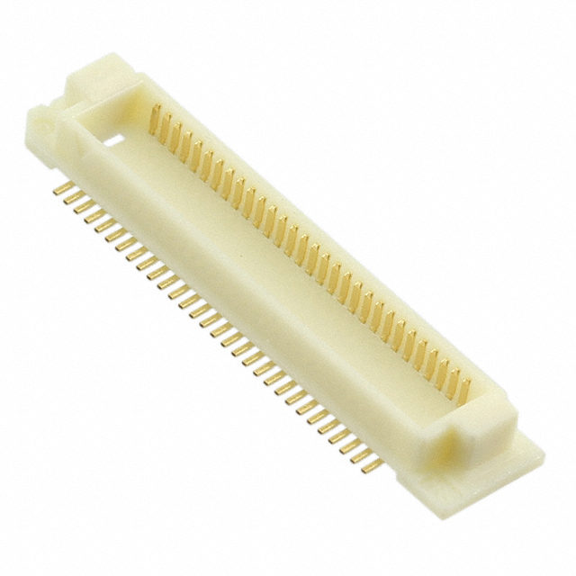
Figure 1: Board Edge Connectors use “fingers” to make contact after slotting into a receptacle. From PCBWay
Figure 2: Right-angle headers like these Amphenol BERGSTIK II make a soldered through-hole connection on one board and slot into a connector on the receiving board. From Amphenol and Digikey
Figure 3: Mezzanine or array connectors like this Hirose FX8 have an arrayed “pinched” connection similar to the board edge connectors, but rely on a mating connector instead of a patterned PCB. From Hirose and Digikey
Each connector type has situations they are best suited for, particularly mechanical factors such as holding power and vibration, as well as signal speed and fidelity of analog signals. In the case of the PSM, I’ll use a right-angle four pin connector for simplicity, but may end up graduating to something like the Hirose FX8 with interleaved ground pins. That said, the cards’ largest component (which will limit the distance between them when stacked) will be the terminals used to connect the rails. Based on maximal current and voltage levels from Table X above, the terminals will likely be Phoenix Contact part number 1135293. Beyond these parameters, the daughtercards will vary by the rails they’re providing voltage and current monitoring of.
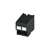
Figure 4: Phoenix Contact part 1135293 These push-button terminals allow access perpendicular to the daughtercard while also avoiding the need to use screwdrivers to fix wires.
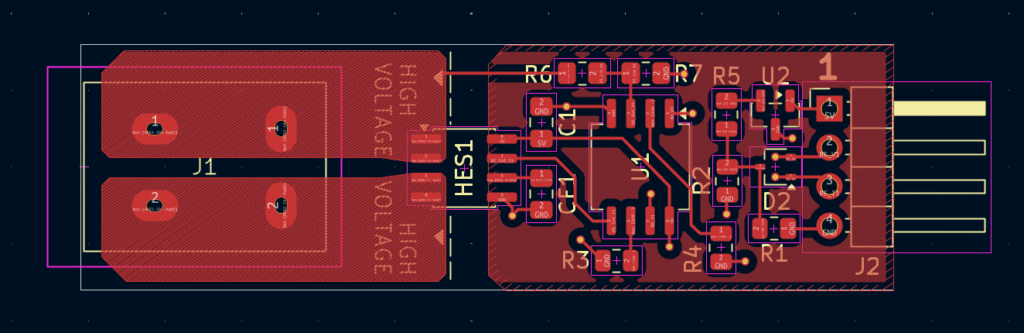
Backend Daughtercard
The backend (BE) daughtercard will monitor the greatest potential voltages and currents on the GARP. For this reason, these cards will include thicker copper layers and a more robust shunt resistor than the cards supporting monitoring the front end (12 and 5 V) rails.
As mentioned, the daughtercards will fulfill two functions:
- Measure voltage on the rail and provide an analog voltage in 0-3.3 V linearly encoding this value
- Measure current consumed on the rail and provide an analog voltage in 0-3.3 V linearly encoding this value
First consider a general design for the voltage measure. A simple voltage divider should be adequate, but based on the prior discussion surrounding the motherboard and MCP3008 ADC ICs, there is a limitation on the maximum value of the resistors used. The alternative is to introduce an op-amp buffer that will provide the reduced impedance needed by the MCP3008’s sample-and-hold ADC. This segment of the circuit can be independent of the current-sensing portion, such that tracewidths can be much smaller.
Two design decisions shape the current sensing portion of the circuit: First, should a high-side or low-side measurement be used, and second, is a Hall-sensor based IC available at the BE rail conditions to provide the current measure, or is a shunt-resistor-based design necessary? Firstly, to avoid lifting the ground the IV DC converters see, a high-side design is used.
As far as a shunt-based design versus dedicated IC, a number of ICs are available to support the shunt design, such as the HV780X series from Supertex. These include a 5x gain on the voltage sensed across the shunt resistor, meaning that to reach 3.3 V at 20 A, the voltage across the shunt resistor would need to be 660 mV and the resistance of the shunt would then need to be 33 mΩ. This would amount to 13.2 W of power consumption at a current consumption of 20 A. While this condition should be rare, it should be possible to produce a Hall sensor-based design with significantly lower power consumption, even at the extremes of the BE rail range.
Similarly, there are many Hall sensor-based ICs available to sense BE current, including the LEM GO series, Allegro ACS71240 series, TI TMCS series, and Allegro ACS713 series. The last of these, the ACS713, provides voltage out in the desired range and can be driven at 5 V. The ACS has a 2100 kV isolation to protect from transients, which should be blocked by the IV DC converters, but this forms a second line of defense. There are 20 A and 30 A range versions of the ACS, with gains/output sensitivities of 185 mV/A and 133 mV/A, respectively. For a maximum of 20 A on the rail, this pushes the output to 2.6 V for the 30 A version (the 20 A version’s output voltage rises to 3.7 V, beyond the 3.3 V input max of the MCP3008 ADC when powered with 3.3 V, as designed herein). For a 10-bit sample, the current resolution then becomes 2.5 mA (neglecting noise introduced by the ACS and other system components) which is a factor of 20 less than the minimum expected current draw on the 80 V rail. The ACS does have a 1.2 mΩ internal resistance, which consumes 24 mW of power at a 20 A draw (more than 500 times less than that of the notional shunt design.)
The current-sensing portion of the circuit will require wider traces, as in the extreme case of full current consumption from the batteries, 20 A will flow through the circuit defined by the terminals, PCB traces, and ACS leads. To evaluate the necessary PCB copper weight and tracewidth, start by assuming the cards/PCBs are fabricated with 1 oz copper traces. To determine if this is sufficient, using (the conservative) IPC-2221, the current carrying capacity of a trace is given by section 6.2:
![\[I = k \Delta T^{0.44} A^{0.725} = k \Delta T^{0.44} w^{0.725} d^{0.725}\]](https://michael-stinger.com/wp-content/ql-cache/quicklatex.com-0b9dec948526f00e515aacf291855282_l3.png "Rendered by QuickLaTeX.com")
Letting  equal 0.048 for an outer board layer,
  equal 10 °C of permissible temperature rise, and a 1 oz Cu trace thickness
  of 35 µm, the trace width required for a 20 A capacity is 66 mm (!). To make this a little more manageable, using a 3 oz copper pour drops this required tracewidth to 6.3 mm. Given that only the terminal and traces to the IC will be potentially subject to this current, this wider tracewidth should be possible without much “art”. Note that the ACS713 uses two SOIC pins per power terminal, such that the power pin pads for input and output define a 1.92+ mm wide area, meaning the traces will need to extend laterally beyond the SOIC footprint.
Intermediate Voltage Daughtercard
The Intermediate voltage (IV) daughtercard will satisfy the same two functions as mentioned previously, namely providing a measurement of voltage and current as an analog voltage in 0-3.3 V. The IV operating at a reduced 24 V opens some additional design options- in particular, shunt-based designs such as using the TI INA199 provides an integrated IC with three gain options to allow minimizing shunt resistance and power consumption. That said, A Hall-based sensor is still expected to provide better isolation of load- and output-side electronics. Estimating a few key metrics for typical Hall-based and shunt-based designs:
| Metric | Hall-Based ACS713 (20 A) | Shunt-Based INA199 w/ 1.3 mΩ shunt |
|---|---|---|
| Power Consumption @ 12.5 A | 188 mW | 206 mW |
| Typical Gain Error % @ 25°C | 1.5% | 1% |
| Output Range | 0-1.25 V | 0-3.3 V |
| Resolution @ 3.3 V / 10 bits | 32.3 mA | 24.7 mA |
| Resolution as % of Table 3 | 18% | 14% |
As can be seen above, the two designs use similar amounts of power at full current as they both incur a similar resistance, either 1.2 mΩ internally for the ACS713, or 1.3 mΩ externally for the INA199. The primary trade then becomes (a) the better resolution of the shunt design given that the shunt resistor is tuned to the desired output range, versus (b) the electrical isolation afforded by the Hall-based design. Comparing the estimated resolution as a function of the minimum expected current draw from Table 3, there is a relatively small difference between the Hall-based and shunt-based designs. As such, and given the additional isolation of the Hall-based design, the IV daughtercard design will use a Hall-based current sensing IC, more specifically, the 20 A variant of the ACS713, the ACS713ELCTR-20A.
For voltage sensing, a simple resistor bridge will be used again to scale the 0-24 V input range to 0-3.3 V. This design is subject to similar impedance considerations as for the backend daugthercard, but with a different divider factor.
Front End Daughtercards
Staying on trend, the frontend (FE) daughtercards can also be made with the same design as the BE and IV cards, using a ACS713 Hall sensor and voltage divider for the current and voltage sensing functions. If the outputs of the ACS713 and voltage divider are used directly, two challenges arise.
First, and particularly with the BE and IV cards, using a voltage divider to bring the native 80 V or 24 V ranges down to 3.3 V will result in either the large currents and power consumption 9 of small resistors (and otherwise desired low impedance), or high impedance that will degrade the performance of the ADC.
Second, the ACS713 has three variants for 5, 20, and 30 A maximum currents, each with a fixed gain, leading to under- or overuse use of the full 0-3.3 V daughtercard output range. Given that the lowest current rail, 12 V is still expected to support up to 5 A, the 20 or 30 A versions will need to be used. The gains for these two variants are fixed as summarized below:
| Rail | BE | IV | FE12 | FE5 |
|---|---|---|---|---|
| Max Current | 20 A | 12.5 A | 5 A | 6 A |
| ACS713 Variant | 30 A | 20 A | 20 A | 20 A |
| ACS Gain | 66 mv/A | 100 mV/A | 100 mV/A | 100 mV/A |
| Max ACS Output | 1.32 V | 1.25 V | 0.5 V | 0.6 V |
| % of 3.3 V Range Used | 40% | 38% | 15% | 18% |
| Gain to Full Range | 2.5 | 2.64 | 6.6 | 5.5 |
Voltage Sensing Circuits
For each of the rails’ voltage sensing circuits, a voltage divider can be used to scale the rail voltage down to the 0-3.3 V range. The voltage divider designs are summarized in Table 6 below. Normally, a trade between power consumption and impedance (as seen by the following ADC) would be considered, but the voltage dividers are expected to be followed by a buffering opamp.
| Rail | BE | IV | FE12 | FE5 |
|---|---|---|---|---|
| Maximum Voltage | 82 | 24 | 12 | 5 |
| Target Divisor | 24.85 | 7.27 | 3.64 | 1.52 |
| R2 | 82 k | 150 k | 330 k | 820 k |
| R1 | 2 M | 1 M | 1 M | 1 M |
| Power Consumption | 3.2 mW | 500 uW | 110 uW | 14 uW |
| Actual Divisor | 25.39 | 7.67 | 4.03 | 2.22 |
| Actual Voltage | 3.2 V | 3.1 V | 3.0 V | 2.3 V |
| Gain to Full Range | 1.03 | 1.06 | 1.1 | 1.4 |
Active Clipping Circuit
As can be seen in Table 5 above, with just the ACS, less than half of the available dynamic range allowed by a 0-3.3 V interface is used. To use the full range (while retaining the isolation afforded by a Hall-based design) a linear gain stage can be appended to the circuit. The voltage divider circuit can also benefit from a linear gain stage, although this is driven by the buffering effect of the opamp output as input to the ADC. To achieve the desired tunable linear gain, an operational amplifier (opamp) can be appended to the circuit in a non-inverting configuration. Furthermore, to also clip the output to a maximum of 3.3 V, two typical options are available:
- Operational Amplifier with 3.3V rail: This clips the output at 3.3 V, but can run into issues reaching the upper rail when output currents are no longer insignificant. This also means the 5 V supplied to the daughtercards will need to be reduced to 3.3 V via (e.g.) a voltage divider, introducing more power consumption.
- Active clipper circuit with reference: By feeding an active clipper circuit with a voltage reference like the REF3033, output can be clipped precisely at 3.3V while supplying the opamp with the native 5 V source.
An active clipper will be used to provide more precise clipping of the output to protect the motherboard’s ADCs without needing to scale the opamp’s supply voltage. The active clipper is a common design as depicted in Figure 5: a non-inverting opamp with a diode and voltage reference added into the feedback loop.
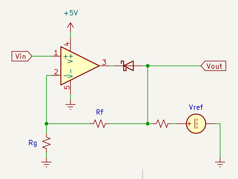
 (assuming is less than 5 V). Keeping the diode in the feedback loop allows the opamp to compensate for the voltage drop across the diode, and powering the opamp above the reference voltage allows the output to clip accurately at .
 For an alpha maturity device, the key design parameter is the resistance in the feedback loop. Using the target gains from Tables 5 and 6, and keeping resistances at or below 200 k:
| Rail | BE | BE | IV | IV | FE12 | FE12 | FE5 | FE5 |
|---|---|---|---|---|---|---|---|---|
| Current | Voltage | Current | Voltage | Current | Voltage | Current | Voltage | |
| Gain to Full Range | 2.5 | 1.03 | 2.64 | 1.06 | 6.6 | 1.1 | 5.5 | 1.4 |
 | 200 k | 0 | 200 k | 0 | 200 k | 0 | 200 k | 68 k |
 | 150 k | 200 | 150 k | 200 | 43 k | 200 | 51 k | 200 |
| Actual Gain | 2.3 | 1.0 | 2.3 | 1.0 | 5.7 | 1.0 | 4.9 | 1.0 |
| Software Gain | 1.07 | 1.03 | 1.13 | 1.06 | 1.17 | 1.10 | 1.12 | 1.04 |
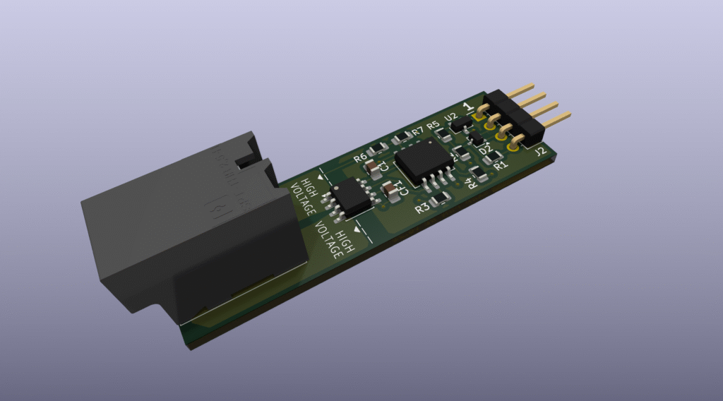
PCB Implementation
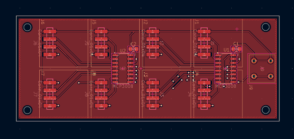
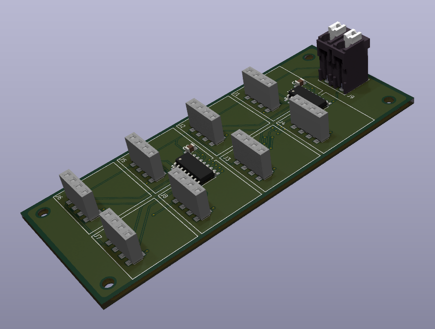
Using the design above, circuit schematics and PCB layouts are made in KiCad. KiCad projects for the GARP are available on GitLab at https://gitlab.com/mvstinger1/ground-autonomy-research-platform/garp-electrical-engineering. Example PCB layouts and models for the motherboard and daughtercards are shown in Figures 6 and 7 below:
Physical Enclosure and Mounting
The key objective of the physical enclosure is in its name- to enclose the PCBs and prevent exposure of electrical components or contacts. Secondarily, the enclosure will help brace the daughtercards and reduce strain on the connectors to the motherboard, particularly when making connections to the power rails.
There are a few key requirements for the PSM’s enclosure. First, I plan to print the parts on my rickety old 3D printer, so parts shouldn’t be too complex. The enclosure will need to provide apertures for the daughtercards’ rail terminals as well as the 5 V power terminal and USB port. The enclosure will also need to attach securely to the DIN rail alongside the other power subsystem components like the DC adapters. Finally, and perhaps most obviously, the enclosure will need to fit within the vertical space defined by the chassis’s frame.
In order to assemble the enclosure, I’ll use threaded inserts for fixing the motherboard to the enclosure, to fix two parts of the enclosure together, and to fix the enclosure to a separate DIN rail mount as I did with the motor controller enclosures. I also expect to use a ribbon cable within the enclosure to route the microcontroller’s USB port to the exterior face.
Other than the above design strategies, the enclosure is fairly simple. As an aside, as began while making the Motor Controller enclosure, I’ve fully migrated away from OpenSCAD to a FreeCAD-based workflow beginning with sketches that are then extruded to form shapes which I combine, modify, and ultimately export to meshes. I’ve found this is more efficient than trying to encode the various parameters in OpenSCAD so that I could make edits and tweaks to the design after drafting. Pictures of the design in FreeCAD and printed prototypes are shown below in Figure 8.
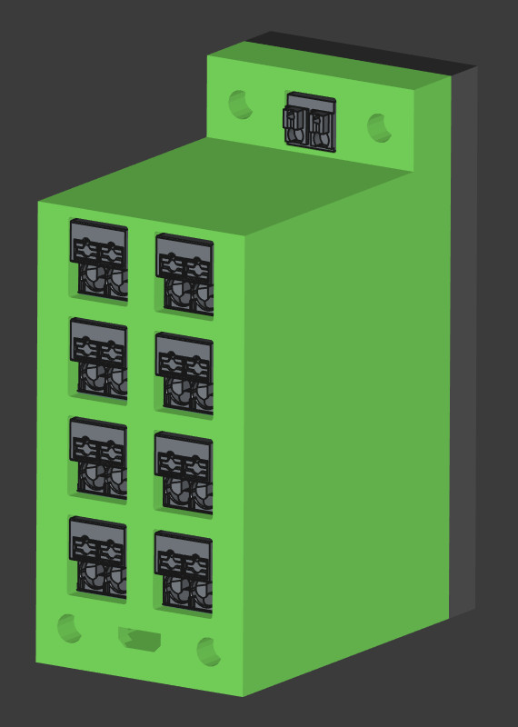
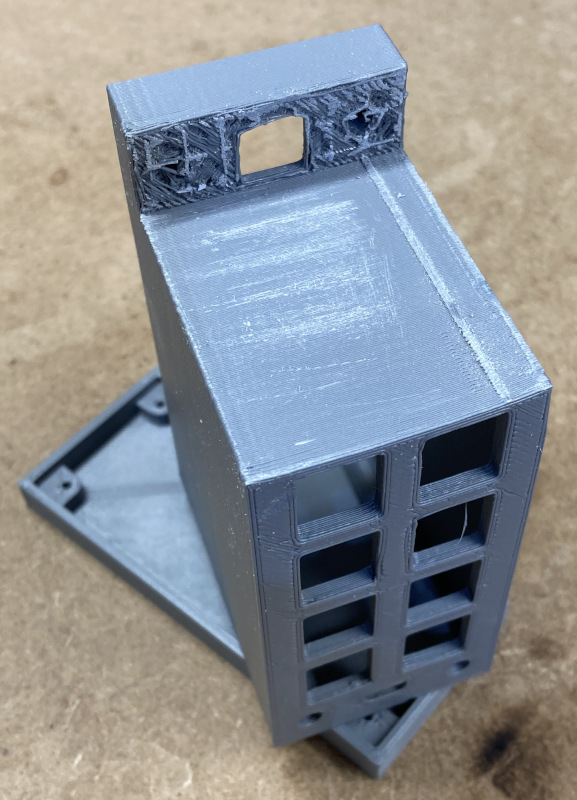
Figure 8: Enclosure render (left) and dimensioning print (right) The PSM enclosure is fairly simple compared to (e.g.) the Motor Controller enclosure, and is primarily a box with cutouts for the daughtercards’ terminal blocks, the main power terminal block, and a USB port. DIN rail mounting is achieved through a printed mount with heat-set threaded inserts screwed to the back of the enclosure.
Next, the firmware for the Power Subsystem is discussed in part two. In this second part, the firmware used to implement the communication controller and ADC controller are discussed. This discussion includes the design considerations in implementing the PSM’s API along with how requests for measurements and the measurements themselves are exchanged between the two cores of the Pico2’s RP2350. It also discusses how the Concise Binary Object Representation (CBOR) data format is used in communication over USB serial and storing the PSM’s configuration in nonvolatile memory (NVM) using a redundant two-bank design for resiliency.
Summary
The Power Subsystem Monitor (PSM) is motivated by the need for reliable, system-wide insight into how power is generated, distributed, and consumed within the GARP. Because nearly every subsystem depends on the power architecture, even subtle voltage or current anomalies can propagate into larger failures. By continuously monitoring key rails, the PSM enables estimation of battery state, detection of abnormal loading conditions, and correlation of power events with system behavior, significantly improving observability and debuggability.
The design targets monitoring of the GARP’s primary power rails—an 80 V backend, a 24 V intermediate rail, and 12 V and 5 V frontend rails—at sampling rates on the order of 10 Hz, sufficient for steady-state characterization. A modular motherboard–daughtercard architecture is used to avoid repeated redesigns as rails or requirements evolve. Each daughtercard is responsible for measuring voltage and current on a single rail and presenting these measurements as analog voltages in a 0–3.3 V range to the motherboard. Centralizing the ADCs and digital logic on the motherboard simplifies layout, allows reuse of a multichannel ADC (MCP3008), and keeps high-power circuitry confined to rail-specific boards.
Hall-effect current sensors are favored across rails to provide galvanic isolation and reduce power dissipation compared to shunt-only solutions, while resistor dividers and buffered gain stages scale rail voltages into the ADC’s input range. Adjustable analog gain and active clipping circuits are used to maximize effective ADC resolution while protecting downstream electronics. PCB design considerations include copper weight and trace width to safely handle worst-case currents, particularly on the backend rail. Sample PCB layouts are presented.
Physically, the PSM is designed to mount on a DIN rail alongside other power subsystem components and is enclosed in a 3D-printed housing that protects the electronics while allowing straightforward wiring access. The article concludes by setting the stage for a second part focused on firmware, including ADC control, inter-core communication on the Pico2, and the use of CBOR for measurement exchange and resilient configuration storage. Sample enclosure images are included.
- https://www.raspberrypi.com/documentation/computers/raspberry-pi.html#power-supply
- https://datasheets.raspberrypi.com/pico/pico-2-datasheet.pdf
- https://datasheets.raspberrypi.com/pico/pico-2-datasheet.pdf
- The 50 mA minimum is truncated from the total power draw (4.25 W at 82 V);
The 50-82 V range is from empirically measuring voltage of a depleted battery - The 175 mA minimum is truncated from total power draw (4.25 W at 24 V, ignoring DC-DC converter losses)
- The 5 A maximum is the point at which the MeanWell DDR-60L-12 is spec’d to shut off output
- The 6 A maximum is the point at which the MeanWell DDR-30L-5 is spec’d to shut off output
- This table is only present in the ‘E’ version of the datasheet; Check the footer of the datasheet- the version ending ‘1295E’ is the first to have this table and recommendations. Or just always go to the manufacturer’s website to collect the newest datasheet.
- Recall electrical power consumption in a resistor is
 while voltage drop in the first resistor in a divider is only
  such that power consumption outpaces voltage drop with increasing current/declining resistance.